Fabrizio Dolcini

Graphene / superconductor junctions
Graphene is a two-dimensional sheet of graphite. Although graphite is a very common material present e.g. in any pencil, scientists believed for long time that it was impossible to ‘extract’ a 2D sheet of it, until the experimental breakthrough by A. Geim and K. Novoselov in 2004 led to the realization of graphene via the mechanical exfoliation technique. The interest in graphene relies on the extraordinary electronic and mechanical properties of this material. In graphene, for instance, it is possible to observe relativistic effects in Condensed Matter materials, where the speed of light is replaced by the Fermi velocity. A. Geim and K. Novoselov in 2004 were awarded the Nobel Prize in Physics in 2010 for their discovery.
References
D. Rainis, F. Taddei, F. Dolcini, M. Polini, and R. Fazio, Andreev reflection in graphene nanoribbons, Phys. Rev. B 79, 115131 (2009).
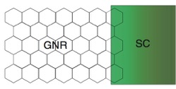
Andreev reflection in a graphene nanoribbon / superconductor hybrid junction
In collaboration with the Research Group of Prof. R. Fazio at Scuola Normale Superiore in Pisa (Italy), we have investigated the phenomenon of Andreev reflection in a graphene nanoribbon contacted to a superconductor.
Models for graphene typically consider an infinitely large 2D sheet (bulk case), which amounts to neglecting the energy scale associated with the finite width of the graphene sample. However, when a graphene ribbon is contacted to a superconductor, such energy scale is in fact of the same order of magnitude (or even bigger) than the Superconducting gap.
Indeed we have shown that finite-size effects lead to notable differences with respect to the bulk-graphene case. At subgap voltages, conservation of pseudoparity, a quantum number characterizing the ribbon states, yields either a suppression of Andreev reflection when the ribbon has an even
number of sites in the transverse direction or perfect Andreev reflection when the ribbon has an odd number of sites. In the former case the suppression of Andreev reflection induces an insulating behavior even when the junction is biased by a voltage; electron conduction can however be restored by applying a gate voltage.
These features remain valid, under some circumstances, also in the case of non-ideal nanoribbons in which the number of transverse sites varies along the transport direction.
Applied techniques
Bogolubov de Gennes Equations